Skip to content
To front page
  • Silicon Wafers 150-200 mm
    • MEMS Wafer Line
      • MEMS SSP and DSP Wafers
      • Selecting the ideal wafer for MEMS devices: Balancing cost, performance, and manufacturing efficiency
    • RFSi® Wafer Line – High Resistivity for RF
      • High Resistivity Wafers
      • Engineered High Resistivity Wafers with Trap-Rich Layer
      • Engineered Ultra High Resistivity wafers
      • UF-RFSi® – Ultra Flat High Resistivity Wafers
      • High Resistivity BSOI Wafers
      • RF GaN Substrate wafers
      • White paper “Advancing from 4G LTE to 5G and 6G: Engineered RFSi® Silicon Wafers for High-Performance RF Devices”
    • Power Wafer Line
      • Power Management SOI wafers
      • Power GaN Substrate wafers (Si and SOI) 
      • Discrete Power Device wafers 
      • White paper: “Enabling next-gen power and RF GaN devices with optimized silicon and SOI substrates” 
    • SOI Wafers – Silicon-On-Insulator Line
      • BSOI Wafers – Bonded SOI
      • C-SOI® Wafers – Cavity SOI
      • E-SOI® Wafers – Enhanced SOI
      • Terrace Free SOI Wafers
    • Patterned Wafers – DRIE and Lithography
    • TSV Wafers – Through Silicon Via
    • DSP Wafers – Double Side Polished
    • SSP Wafers – Single Side Polished
    • EPI Wafers – Epitaxial Silicon Wafers
    • Customized Wafers and Prototyping
    • Production and Capacity Expansion 
    • Supplier Awards and Collaboration Projects
  • Silicon wafers 300 mm
    • Polished silicon wafers 
    • Epitaxial (EPI) silicon wafers 
    • Test and monitor silicon wafers 
  • Applications
    • MEMS and Sensors
    • RF Filters and Devices
    • Power Devices
  • Quality
    • Certificates
    • Quality Policy
    • Quality Tools
      • Artificial Intelligence at Okmetic
      • 5S at Okmetic
  • Sustainability
    • Sustainability Report and Certificates
    • Environment and Targets
    • Responsibility for Personnel
    • Responsibility for Health and Safety
    • Business Ethics
    • Managing Responsibility
  • Work with Us
    • Production Experts
    • Semiconductor Professionals
    • Students
    • Maintenance professional
    • Technical professionals
    • Sales and technical support
    • Open Positions
  • About Okmetic
    • Company
    • Strategy and Values
    • Executive Management Group
    • Investments
    • Research and Development Work
    • Tale of a Silicon Wafer
    • The History of Okmetic
    • News & Insights
    • Contact Us
  • English
    • Suomi
    • 日本語
    • 中文 (中国)

News & insights

Okmetic+About Okmetic+News & insights

Select content category
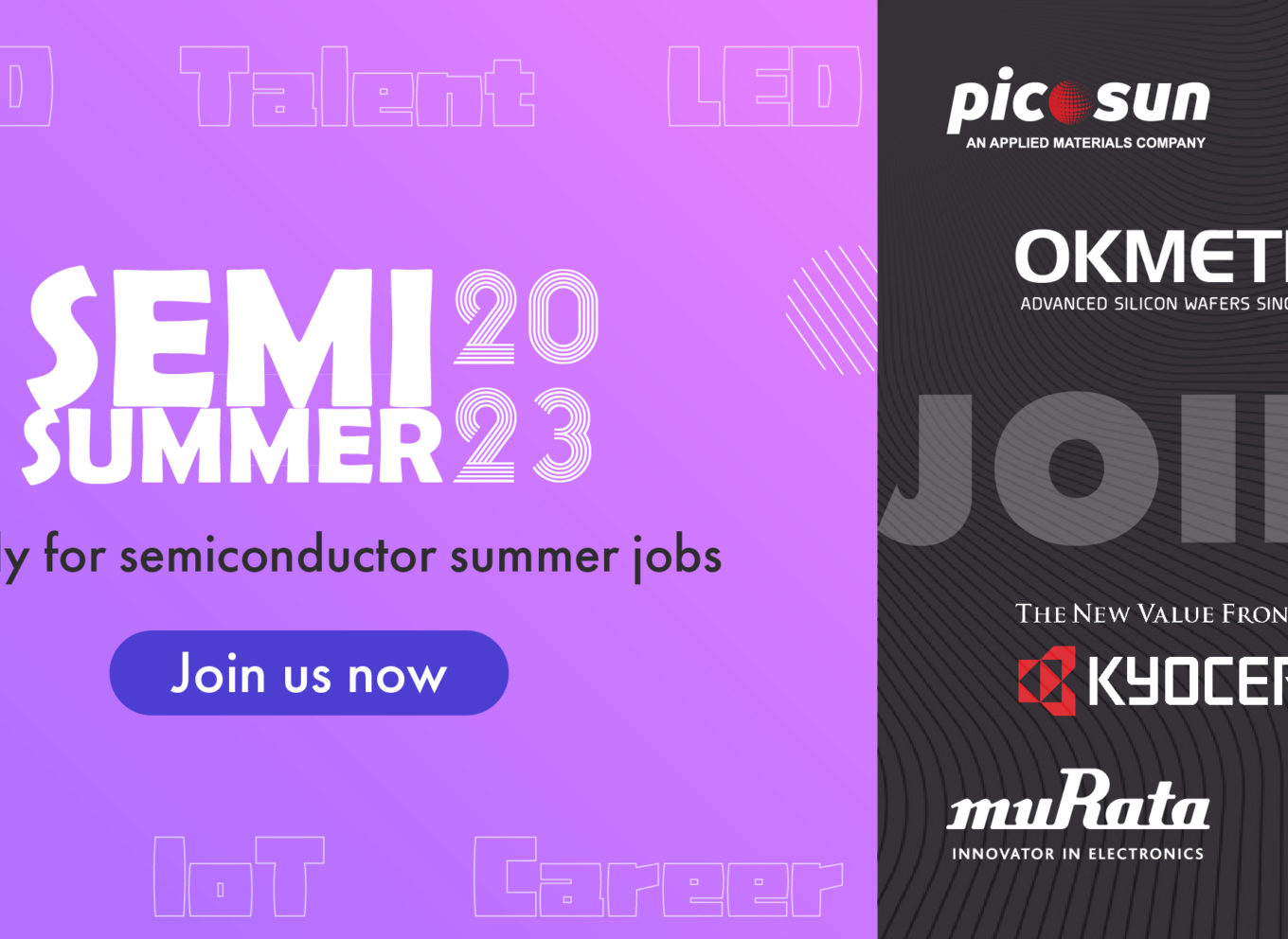
  • Career stories
  • Events
  • Insights
  • News
  • Product news

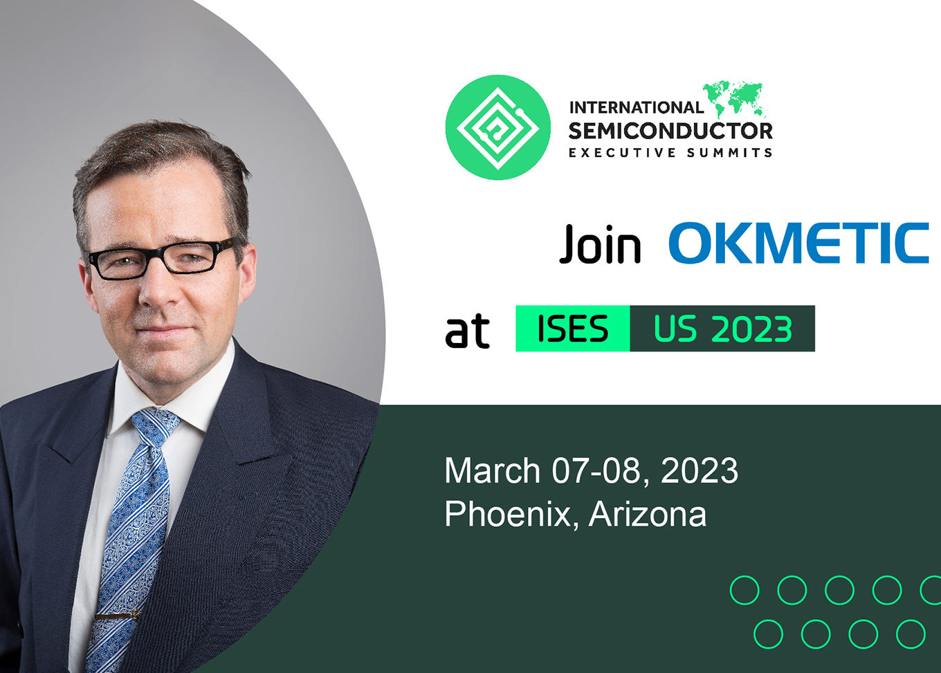
Okmetic CTO Atte Haapalinna to give a presentation at ISES USA 2023

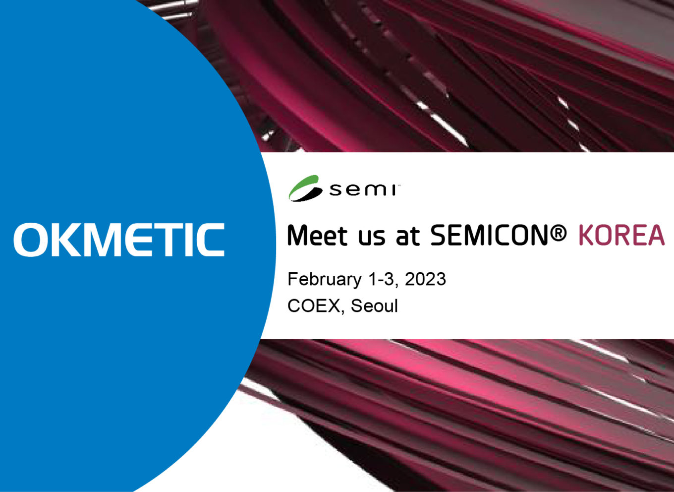
Okmetic is participating SEMICON® KOREA during February 1-3, 2023

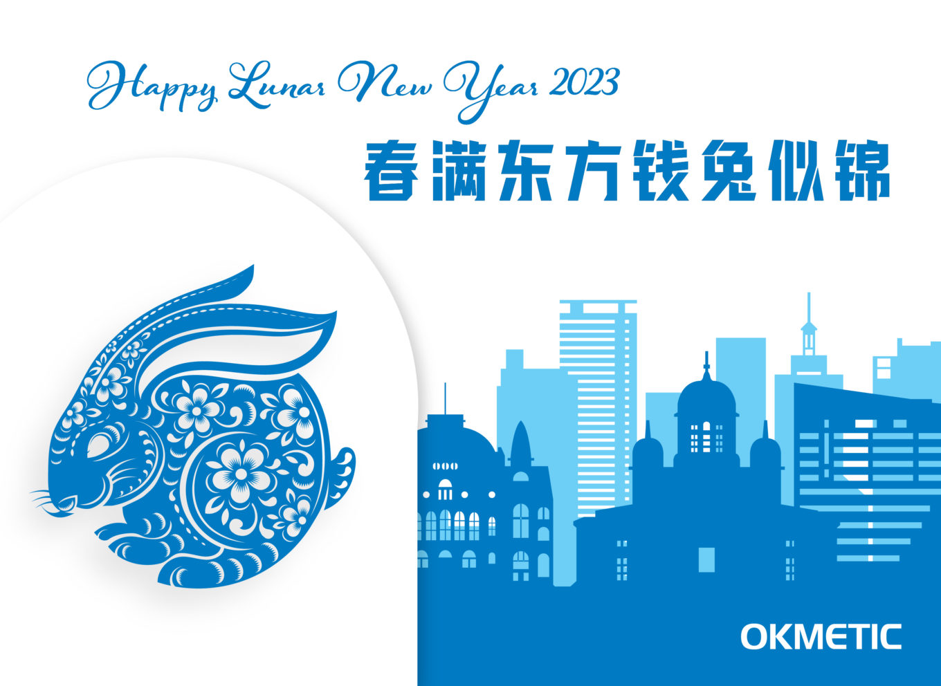
Happy Lunar New Year 2023

Okmetic renewed its values

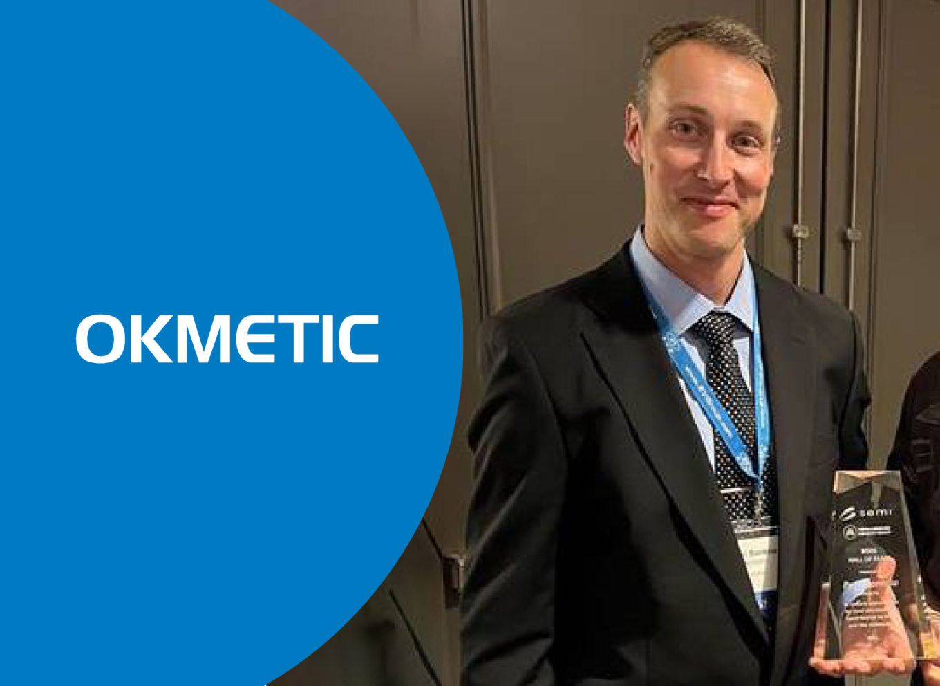
Okmetic Customer Support Manager Petri Santala inducted in the SEMI-MEMS & Sensors Industry Group Hall of Fame

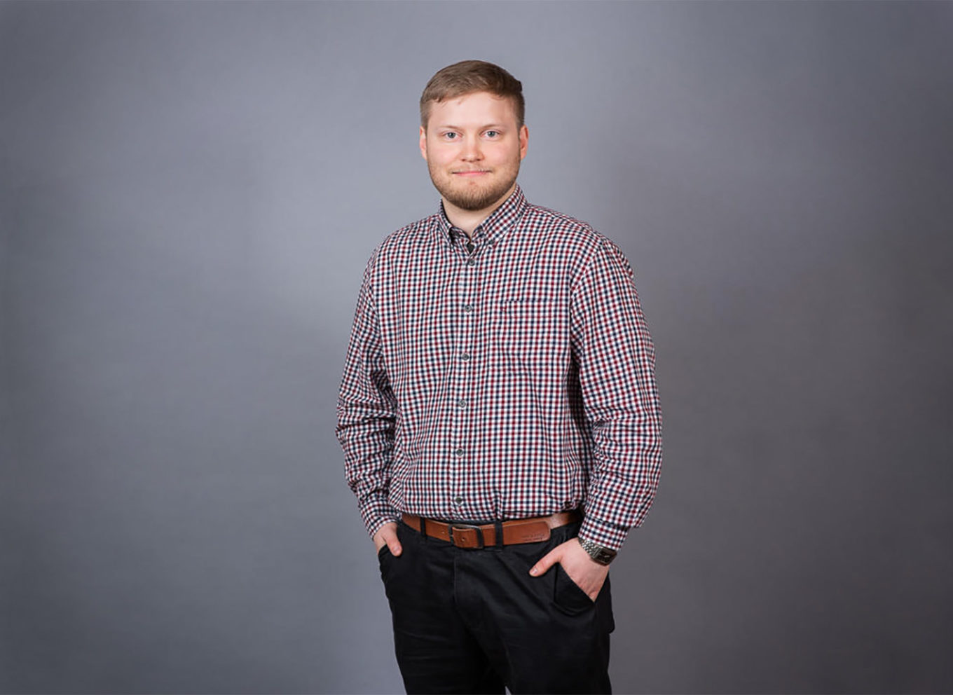
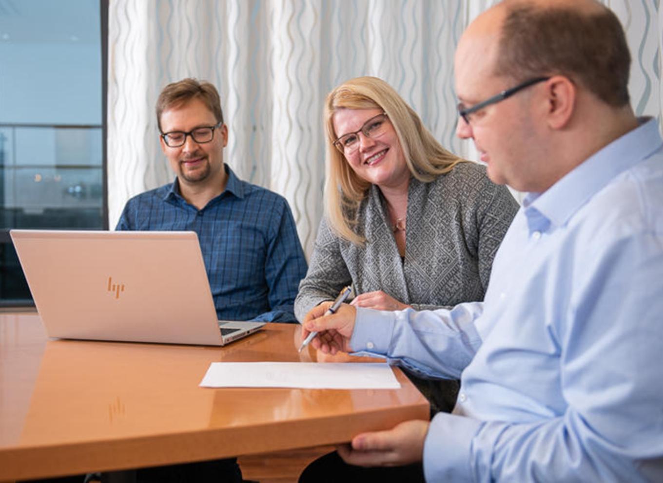
Jonne Vähänissi: “Okmetic is the best place for a process development engineer to work in Finland.”

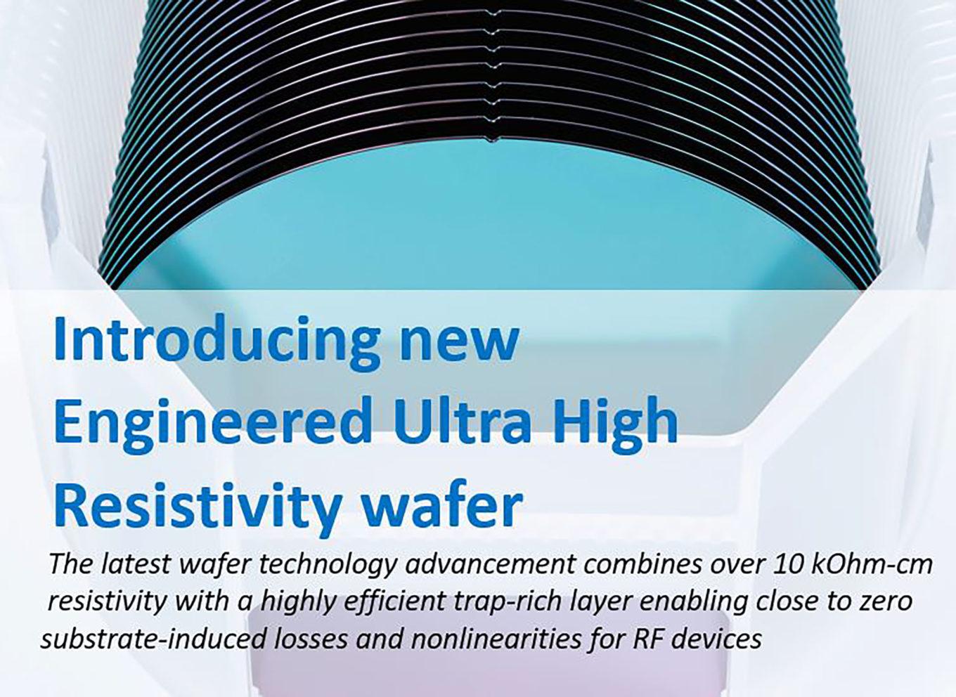
Okmetic Expands Its RFSi® Portfolio with Engineered Ultra High Resistivity Wafer

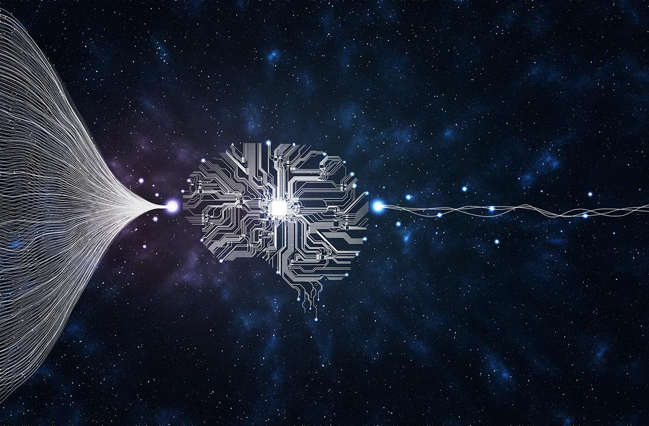
Okmetic On-Demand Webinar: Improving the quality of electronics components and systems with AI

Okmetic participated in Position II project developing next generation smart catheters and implants 

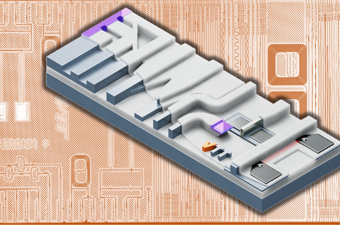
VTT finds Okmetic E-SOI® wafers highly beneficial platform for its Photonics Technology

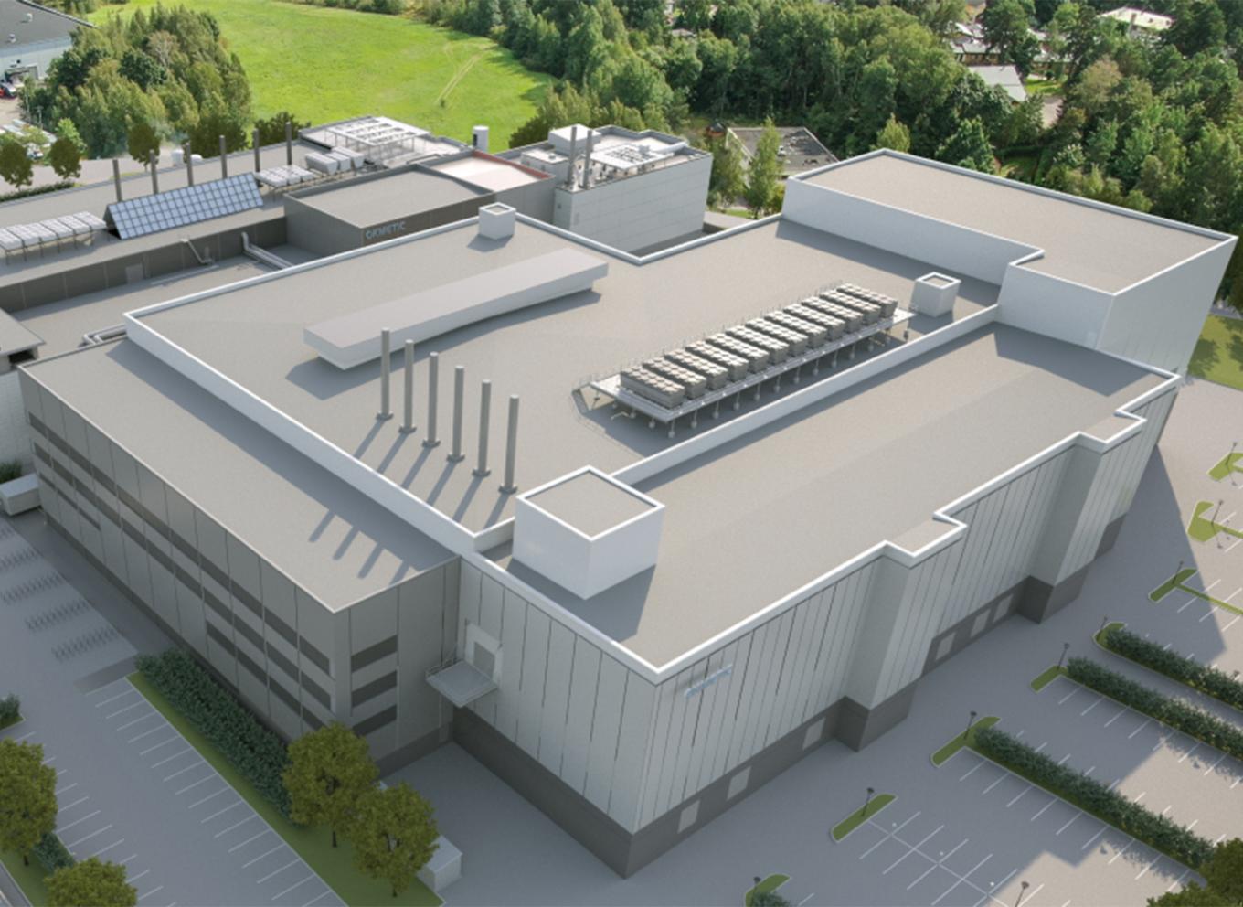
Silicon wafer manufacturer Okmetic invests nearly 400 million euros to build a new fab in Finland with aims to more than double the production capacity and business

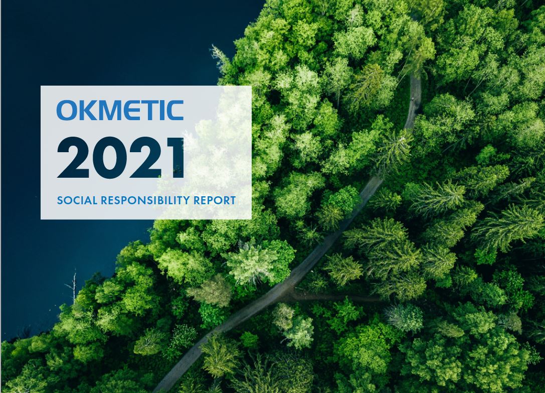
The Social Responsibility Report for 2021 has been published

Okmetic sponsoring MEF Japan on 20-21 April

Artificial intelligence project provides tools for silicon wafer inspection – rare deviations can be detected even in larger data samples

Research paper “Characterization of Heavily Irradiated Dielectrics for Pixel Sensors Coupling Insulator Applications” out now

  • Previous
  • 1
  • 2
  • …
  • 5
  • 6
  • 7
  • 8
  • 9
  • 10
  • 11
  • Next
  • Column
    • Silicon Wafers 150-200 mm
    • Silicon Wafers 300 mm
    • Applications
To front page
  • About Okmetic
  • Contact Us
  • Quality
  • Sustainability
  • Work with Us
  • Privacy Policy and Terms of Use
  • Safety Data Sheet
LinkedIn YouTube WeChat Facebook