News & insights
Select content category
Thank you for 2023

AI to enhance wafer quality and semiconductor device reliability
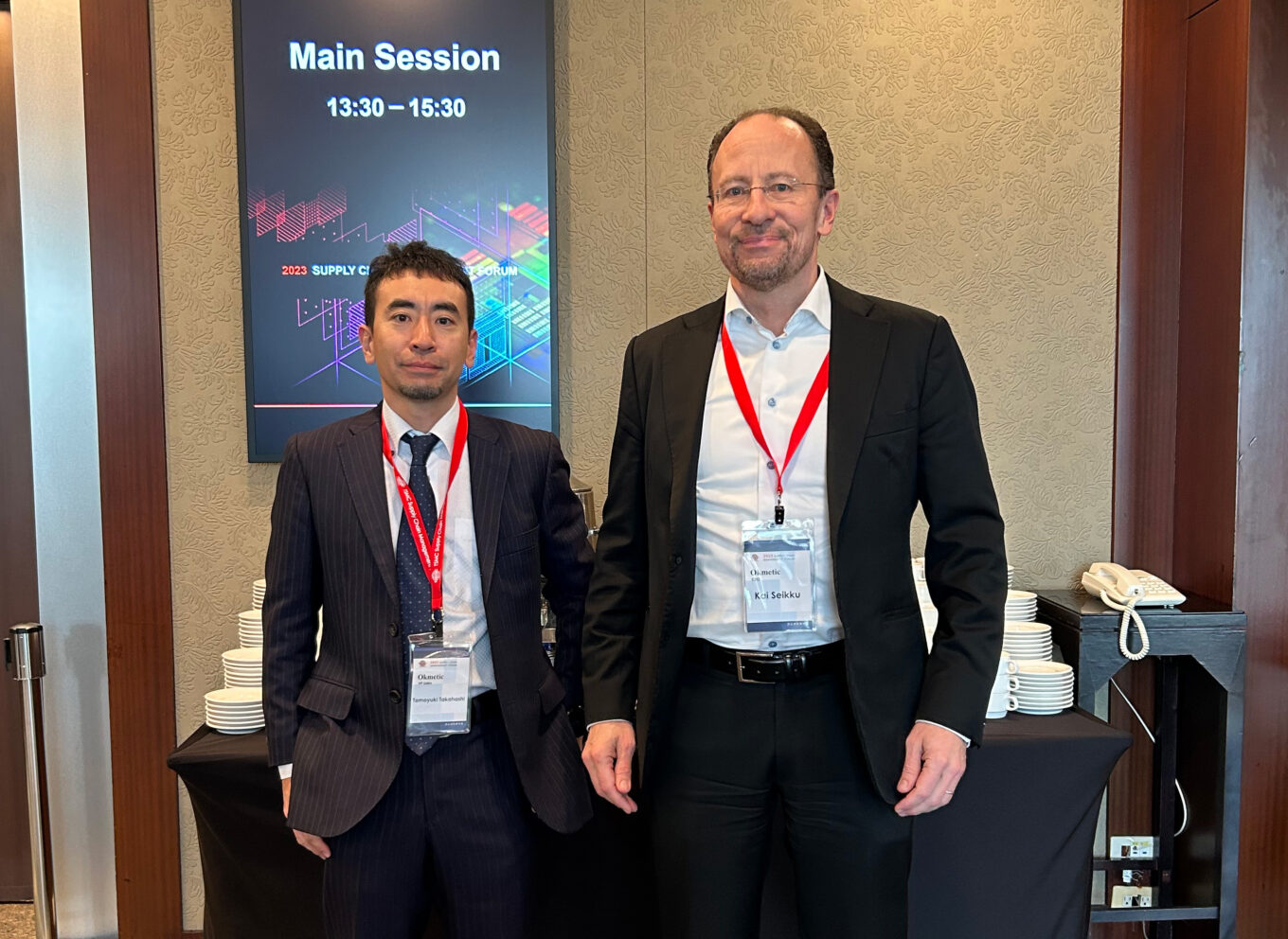
Okmetic participated in TSMC supply day
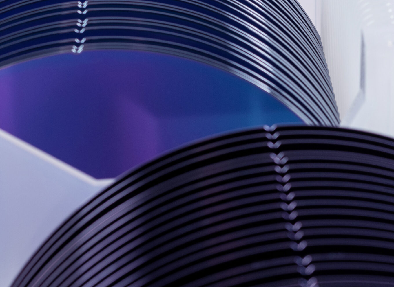
Power wafer line provides optimized substrate solutions for the growing market
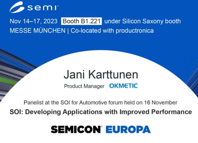
Okmetic participating in Semicon Europa
Heikki Holmberg from Okmetic has been selected as Aalto University School of Electrical Engineering Alumnus of the Year
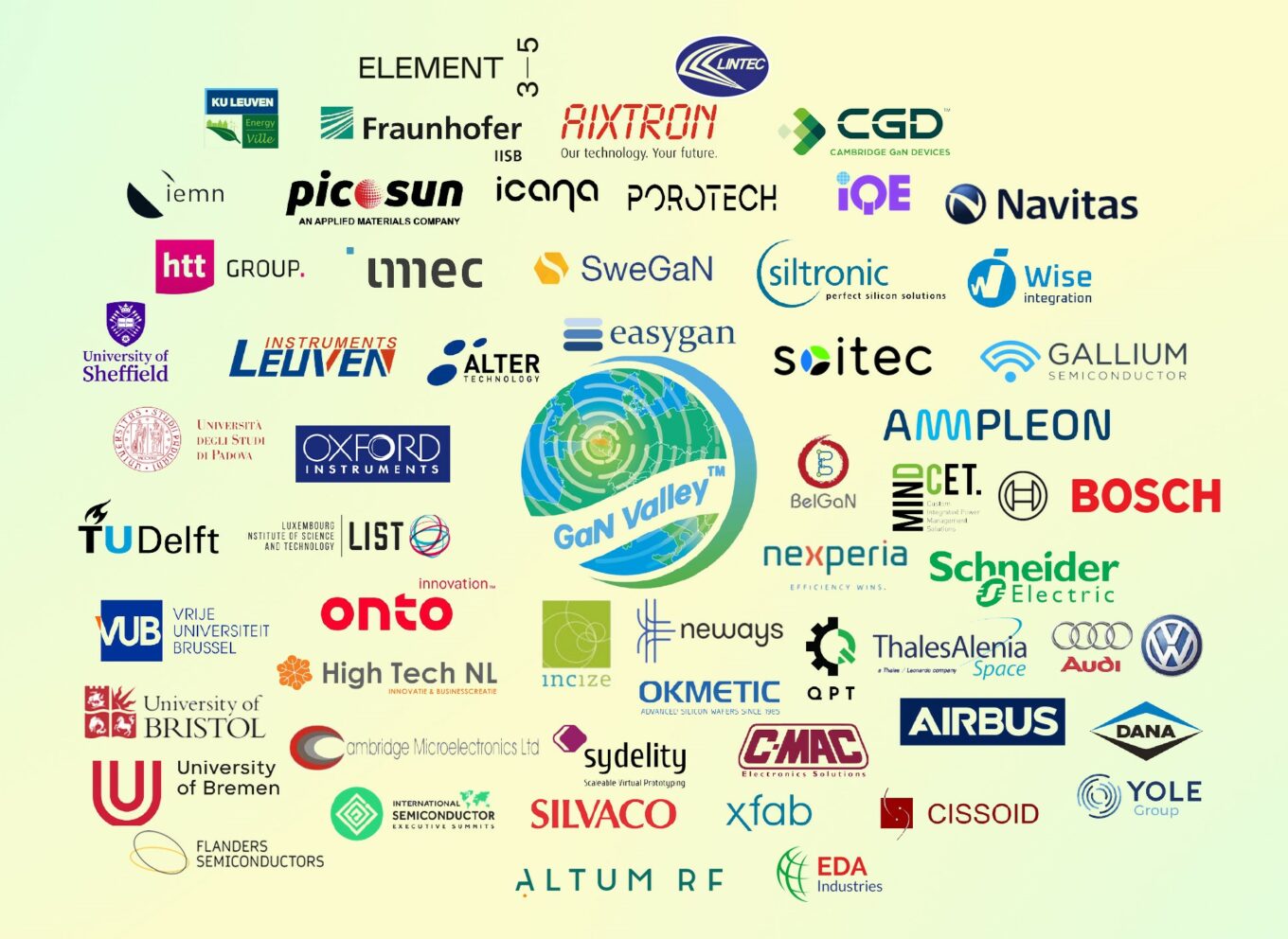
Okmetic is now member of the GaN Valley™
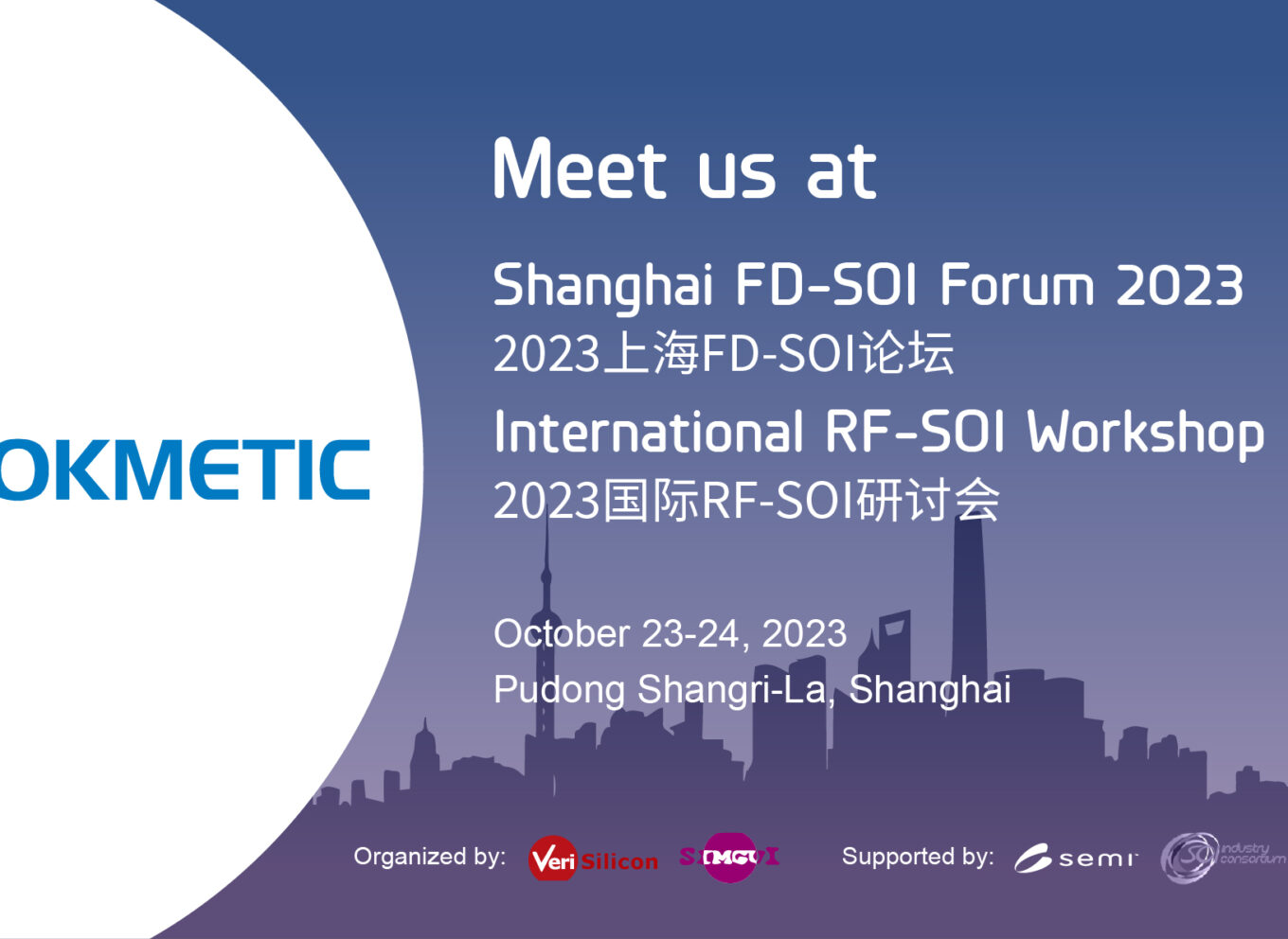
Okmetic is participating Shanghai FD-SOI Forum and 2023 International RF-SOI Workshop
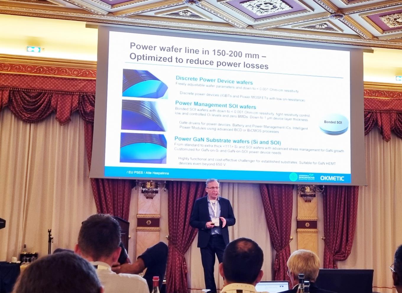
CTO Atte Haapalinna presented Power wafer line at EU PSES
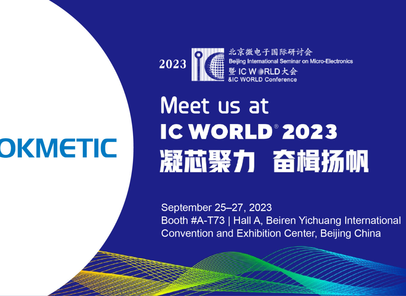
Okmetic is participating 2023 IC WORLD Conference in Beijing during September 25-27
Okmetic enables academic research within the company with the help of Research Impact Foundation
Tuomas Itkonen is appointed Chief Financial Officer
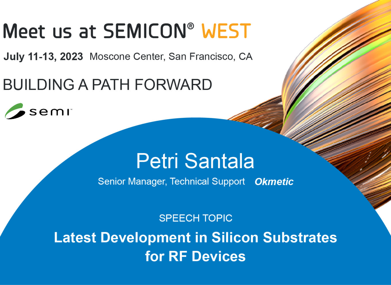
Petri Santala speaking Latest development in silicon substrates for RF devices at Semicon West 2023
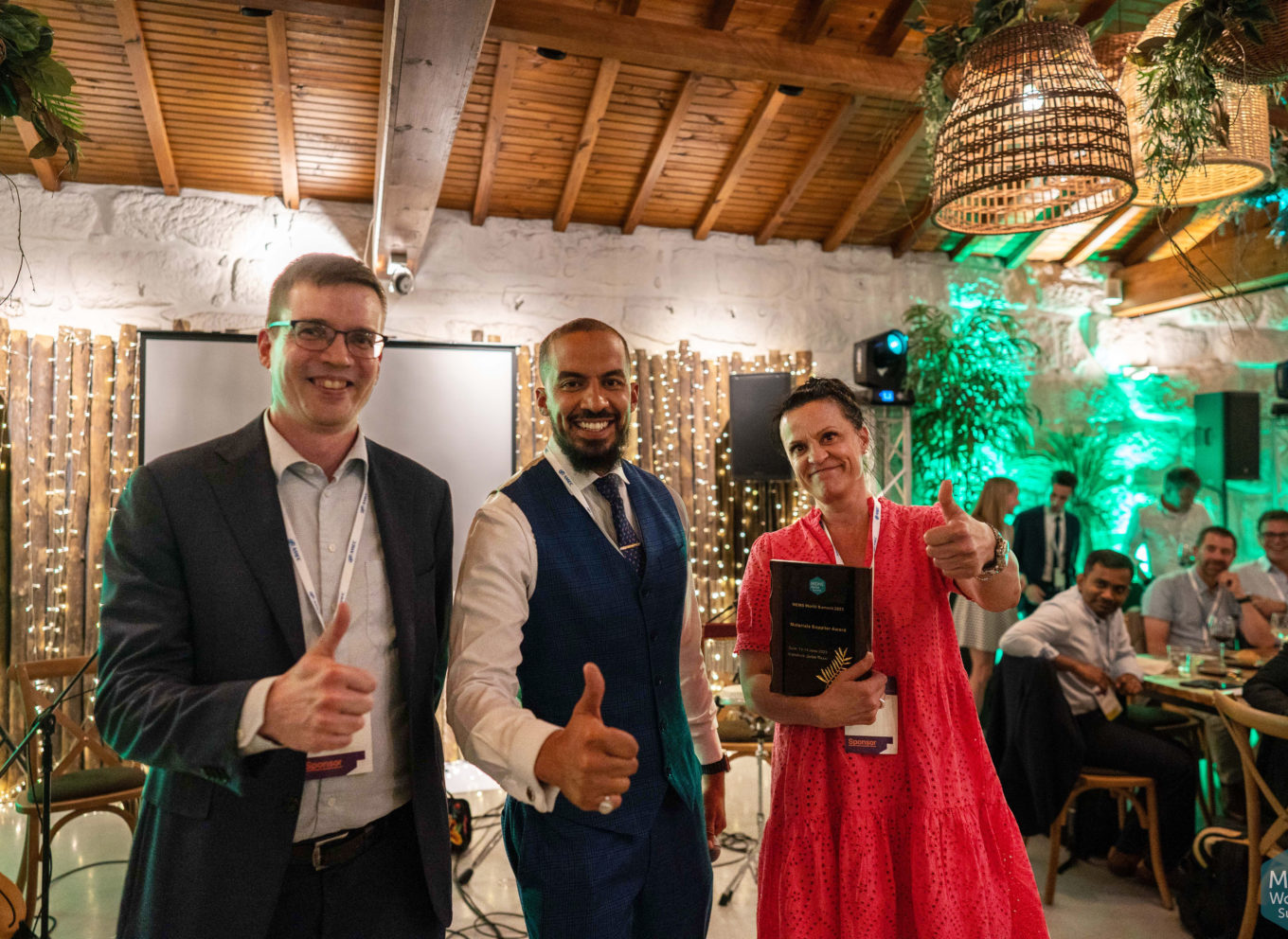
Okmetic has received the MWS Material Supply Award