Skip to content
To front page
  • Silicon Wafers
    • MEMS Wafer Line
      • MEMS SSP and DSP Wafers
      • Selecting the ideal wafer for MEMS devices: Balancing cost, performance, and manufacturing efficiency
    • RFSi® Wafer Line – High Resistivity for RF
      • High Resistivity Wafers
      • Engineered High Resistivity Wafers with Trap-Rich Layer
      • Engineered Ultra High Resistivity wafers
      • UF-RFSi® – Ultra Flat High Resistivity Wafers
      • High Resistivity BSOI Wafers
      • RF GaN Substrate wafers
    • Power Wafer Line
      • Power Management SOI wafers
      • Power GaN Substrate wafers (Si and SOI) 
      • Discrete Power Device wafers 
    • SOI Wafers – Silicon-On-Insulator Line
      • BSOI Wafers – Bonded SOI
      • C-SOI® Wafers – Cavity SOI
      • E-SOI® Wafers – Enhanced SOI
      • Terrace Free SOI wafers
    • Patterned Wafers – DRIE and Lithography
    • TSV Wafers – Through Silicon Via
    • DSP Wafers – Double Side Polished
    • SSP Wafers – Single Side Polished
    • Customized Wafers and Prototyping
    • Production and Capacity Expansion 
    • Supplier Awards and Collaboration Projects
  • Applications
    • MEMS and Sensors
    • RF Filters and Devices
    • Power Devices
  • Quality and Responsibility
    • Quality
      • Quality Policy
      • Quality Tools
        • Artificial Intelligence at Okmetic
        • 5S at Okmetic
    • Sustainability
      • Responsibility for Personnel
      • Responsibility for Safety and Health
      • Responsibility for Environment
      • Business Ethics
      • Managing Responsibility
      • Reports on Responsibility
    • Certificates
  • Work with Us
    • Production Experts
    • Semiconductor Professionals
    • Students
    • Maintenance professional
    • Technical professionals
    • Sales and technical support
    • Open Positions
  • About Okmetic
    • Company
    • Strategy and Values
    • Executive Management Group
    • Investments
    • Research and Development Work
    • Tale of a Silicon Wafer
    • The History of Okmetic
    • News & Insights
    • Contact Us
  • English
    • Suomi
    • 日本語
    • 中文 (中国)

News

Okmetic+About Okmetic+News & insights+News

Select content category

  • Display all
  • Career stories
  • Events
  • Insights
  • Product news

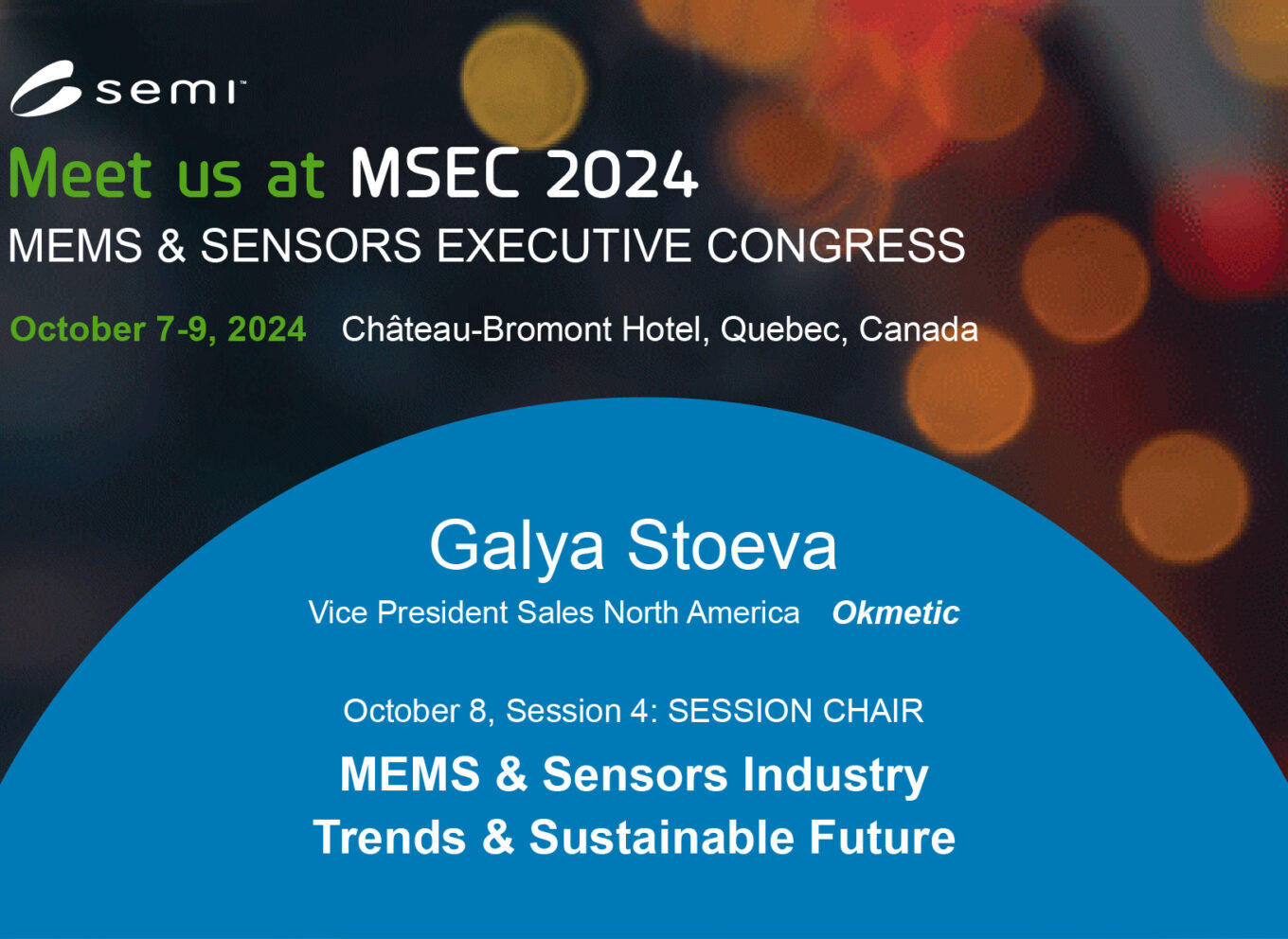
Okmetic is participating in MSEC

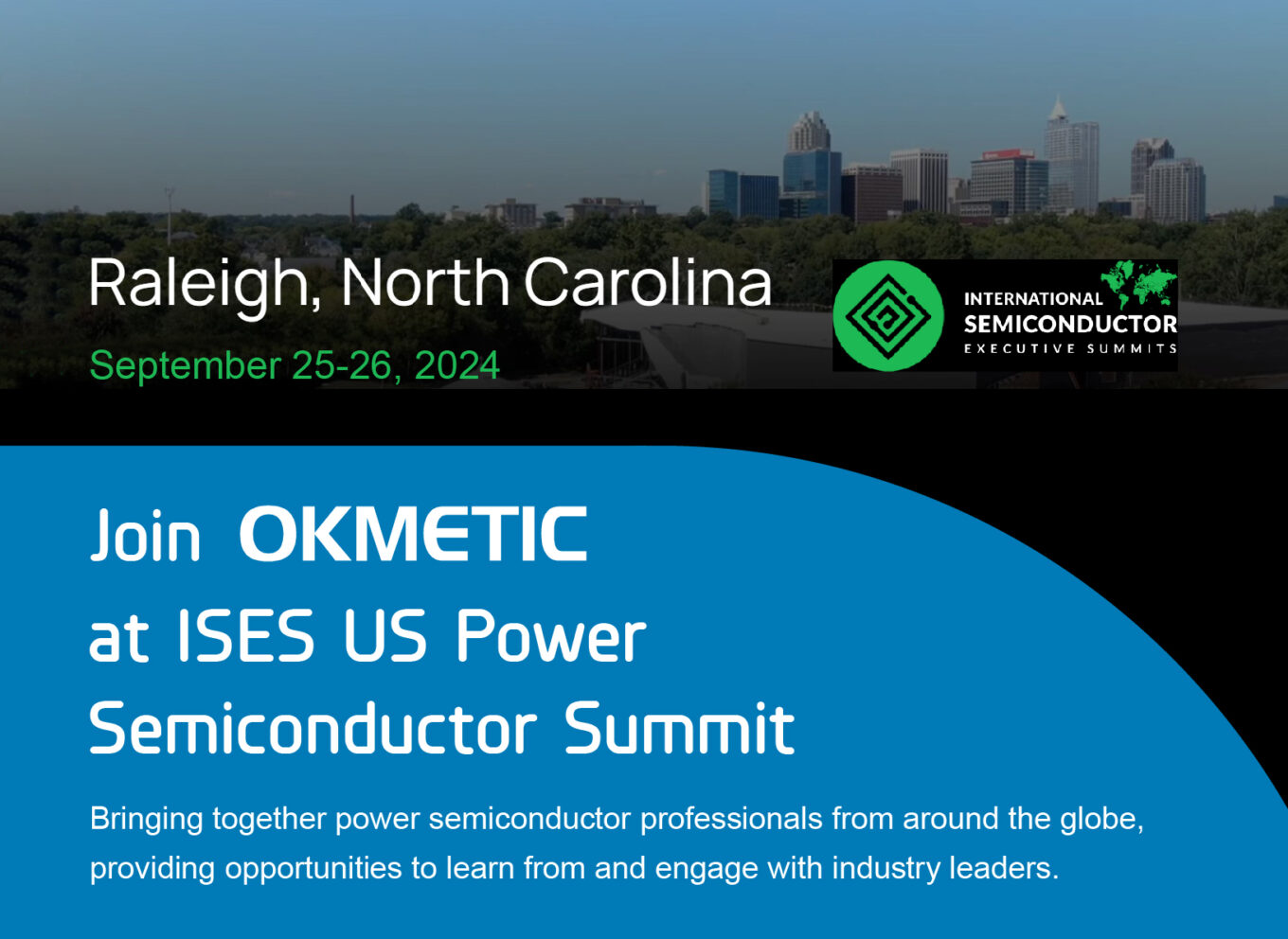
Okmetic will be participating in ISES US Power

Okmetic participates in the ECSA project to respond to the shortage of semiconductor professionals

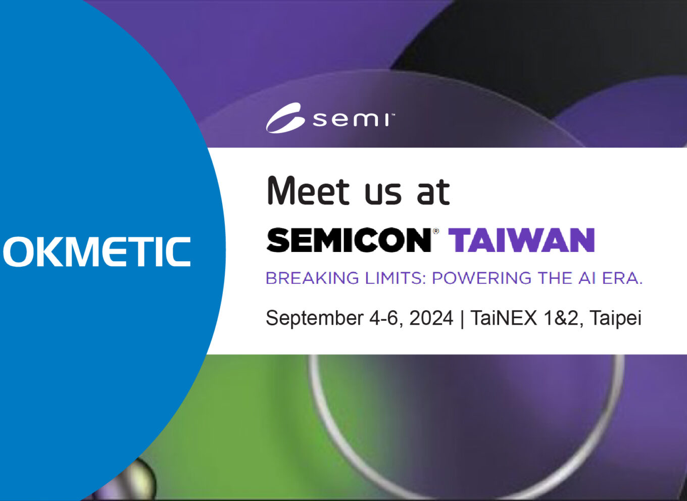
Okmetic is participating in SEMICON Taiwan

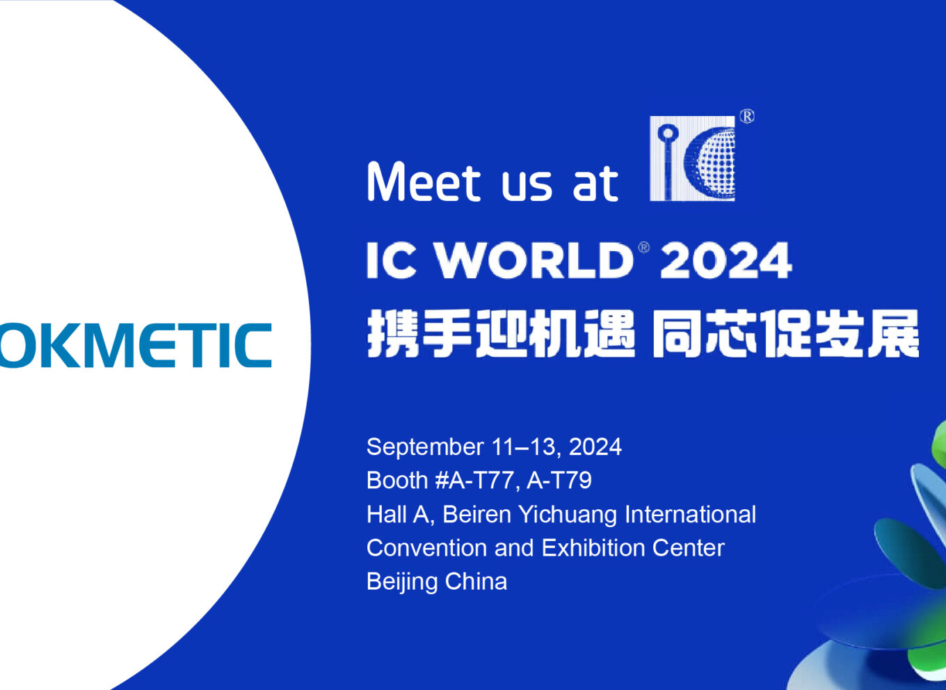
Okmetic participating Beijing Microelectronics International Symposium

Okmetic commits to Science Based Targets Initiative (SBTi) to strengthen its sustainability work

The Sustainability Report for 2023 has been published

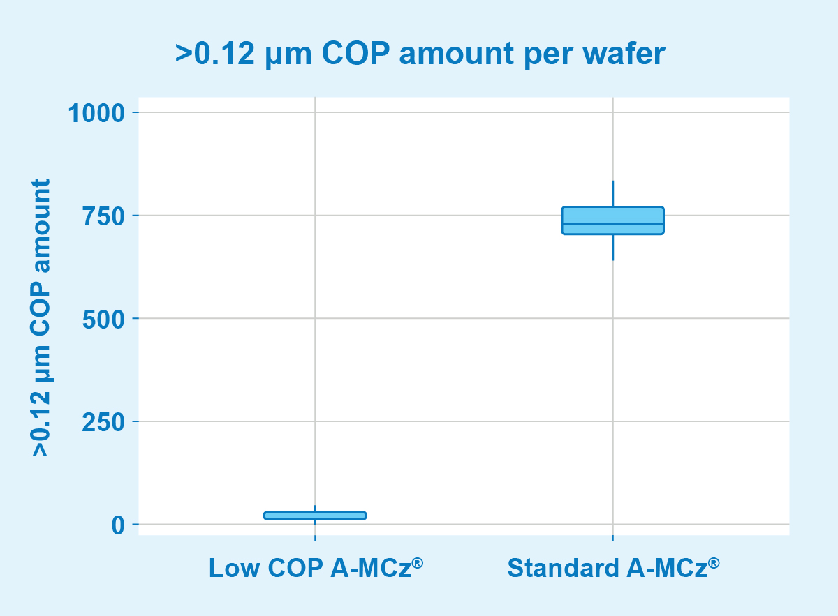
COP level management enhancing power device reliability and yield

New strategy outlines growth opportunities for Finnish semiconductor industry

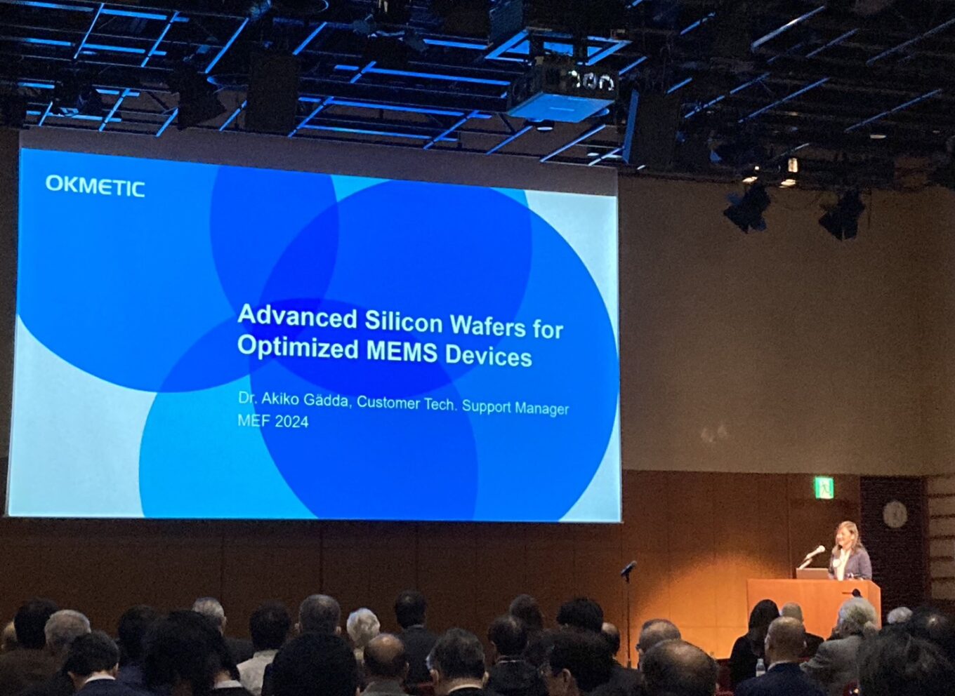
Dr. Akiko Gädda gave a speech at the MEF

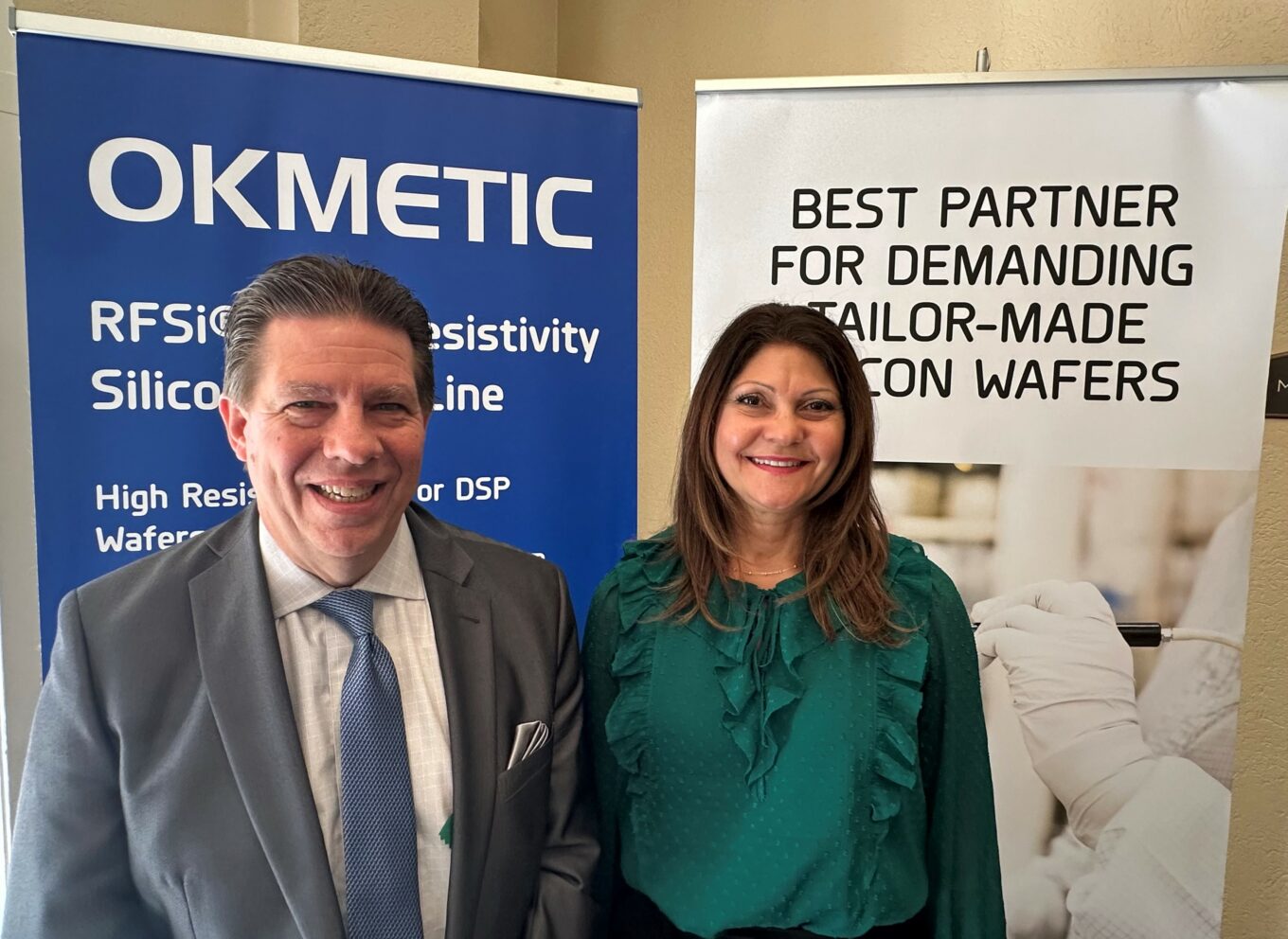
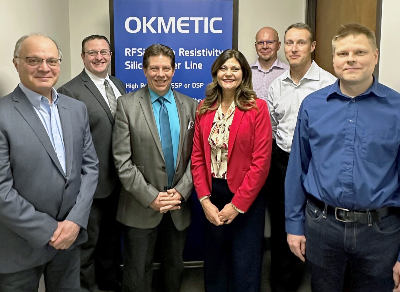
Okmetic participated in CMC Techcet event

Okmeticin Pohjois-Amerikan myyntitiimi

Okmetic Inc. has achieved a 25 year milestone

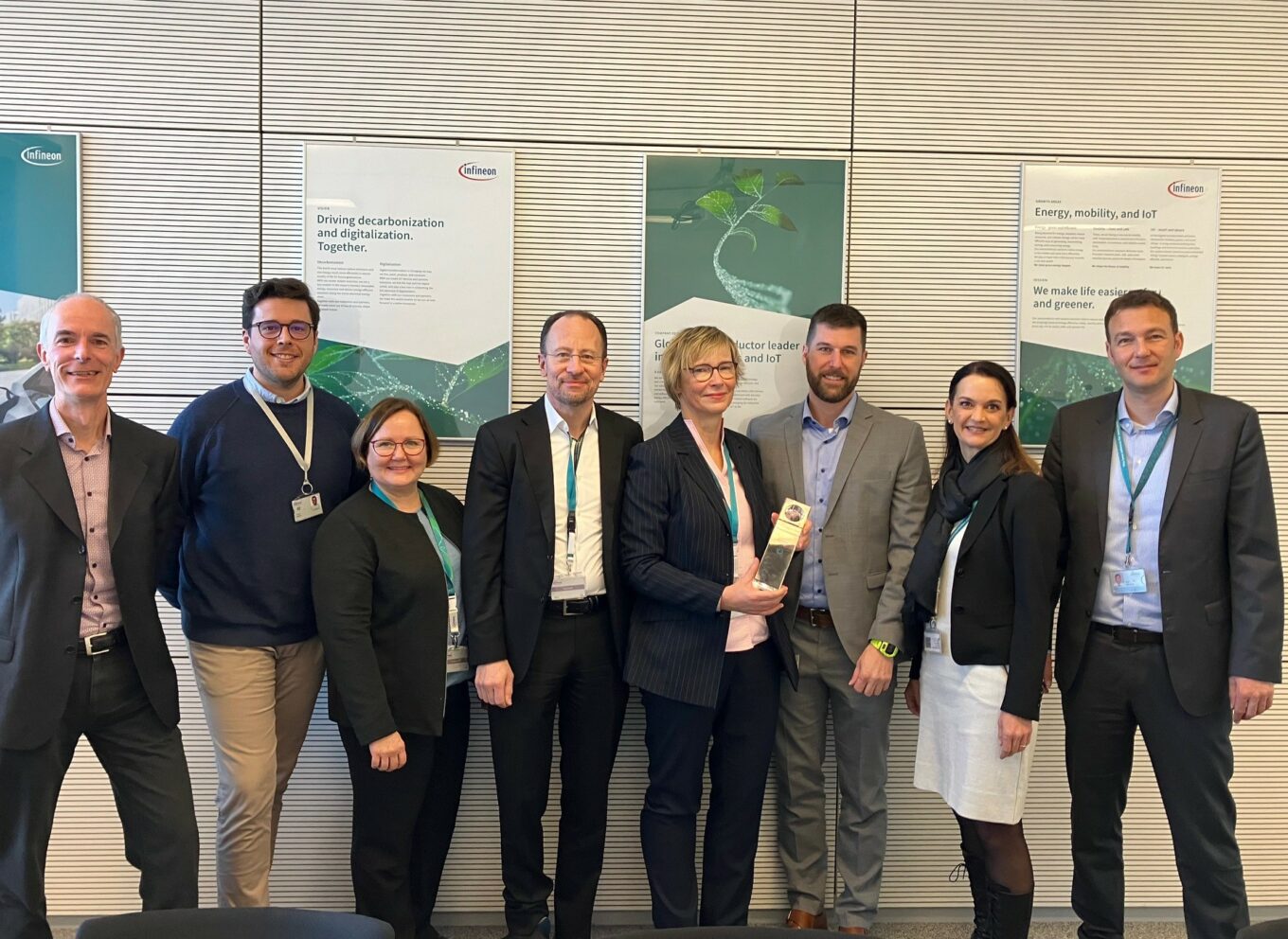
Okmetic receives Infineon’s Best Wafer Supplier award 2023

Okmetic recertified to conform to IATF 16949:2016 standards

Happy Lunar New Year 2024

  • Previous
  • 1
  • 2
  • 3
  • 4
  • 5
  • …
  • 7
  • 8
  • Next
  • Silicon Wafers
    • Column
      • SOI Wafers – Silicon-On-Insulator Line
      • Patterned Wafers – DRIE and Lithography
      • TSV Wafers – Through Silicon Via
    • Column
      • RFSi® Wafers – High Resistivity Line for RF
      • SSP Wafers – Single Side Polished
      • DSP Wafers – Double Side Polished
    • Column
      • Power wafer line
      • Customized Wafers and Prototyping
      • Production and Subcontracting
To front page
  • About Okmetic
  • Contact Us
  • Applications
  • Quality and Responsibility
  • Work with Us
  • Privacy Policy and Terms of Use
  • Safety Data Sheet
LinkedIn YouTube WeChat Facebook