News
Select content category
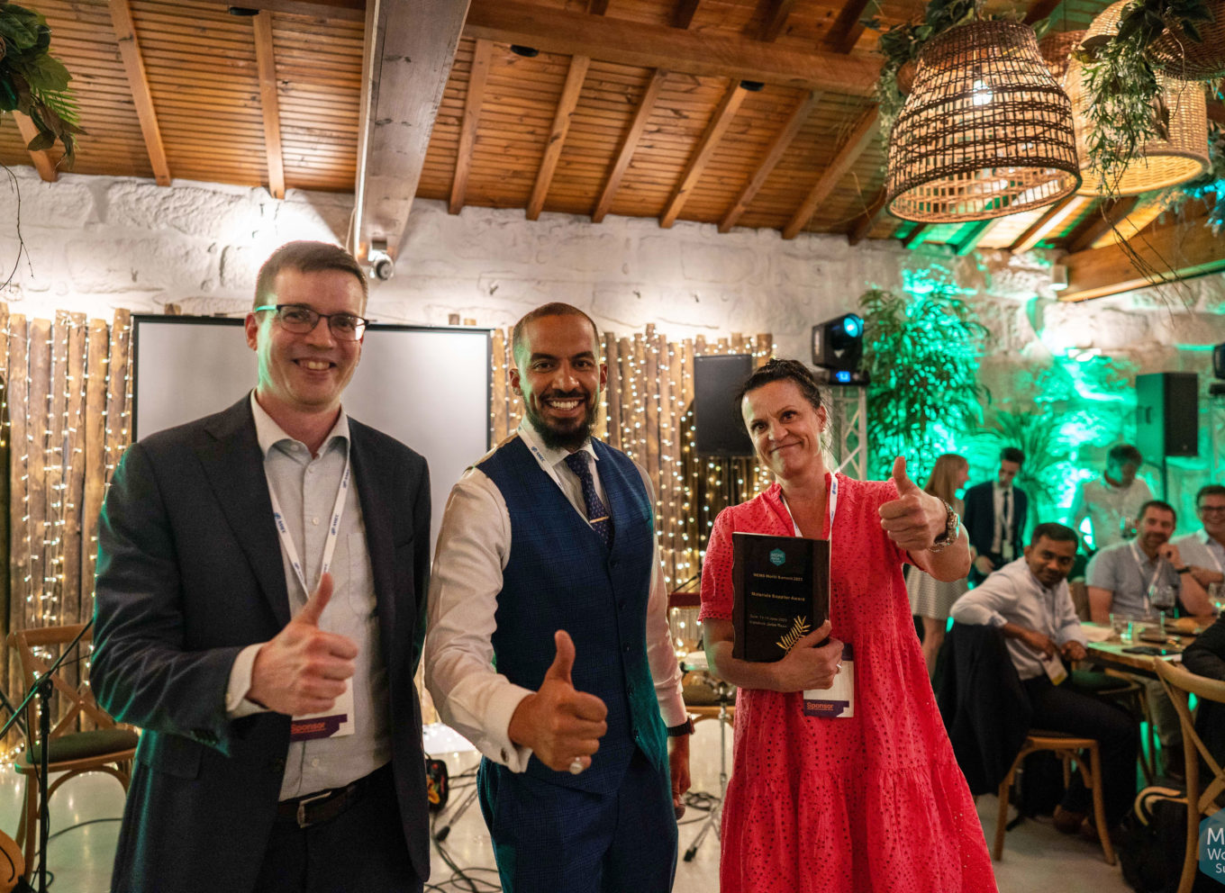
Okmetic has received the MWS Material Supply Award
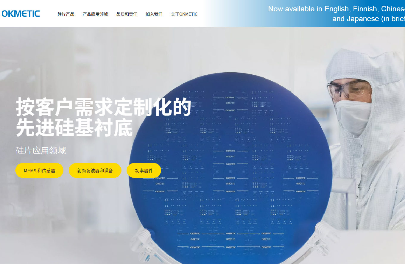
Okmetic.com/zh/ now provides more content in Chinese
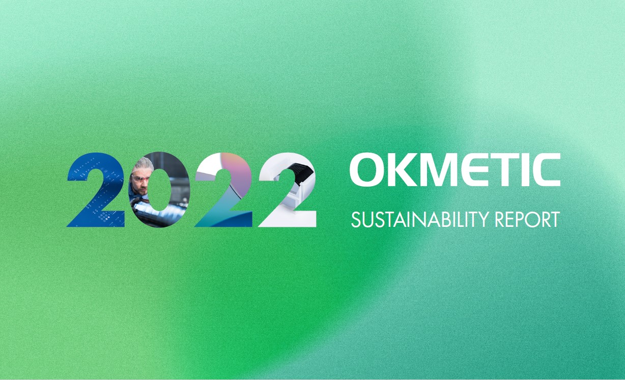
The Sustainability Report for 2022 has been published

Okmetic partaking in RF themed R&D project consortium
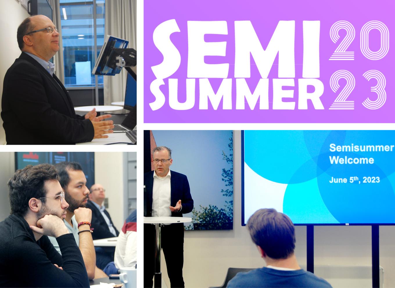
Semi-Summer 2023 is now launched
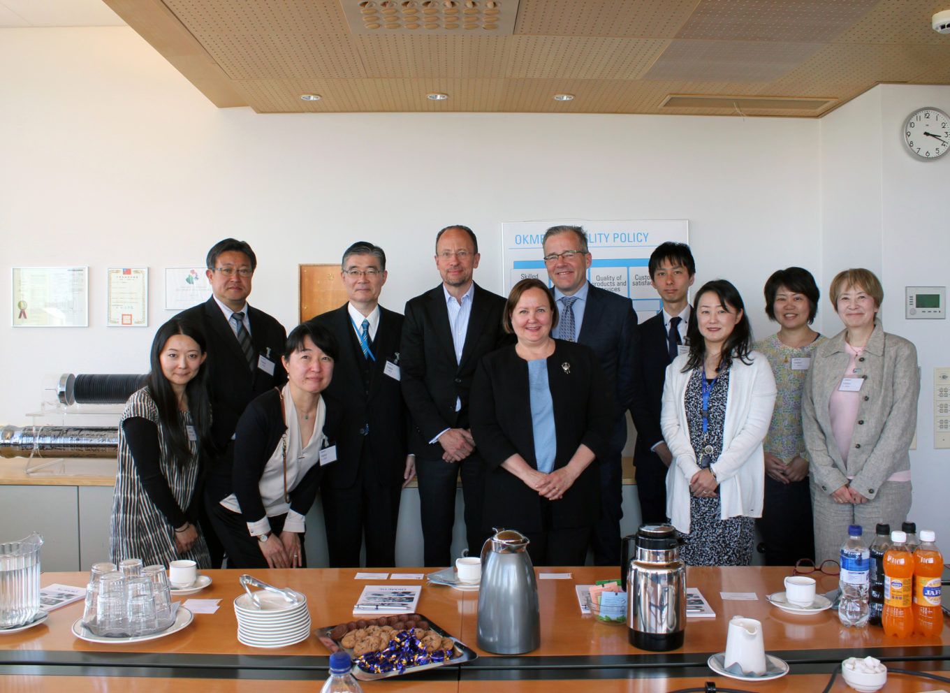
We had the honor to have Ambassador of Japan, Kazuhiro Fujimura, visit Okmetic on May 29
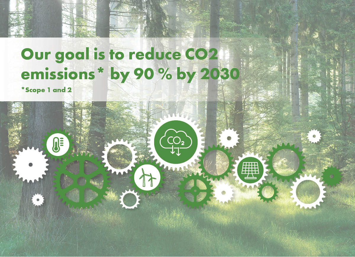
We have set a target for our greenhouse gas emissions

Okmetic’s responsible operations have been audited
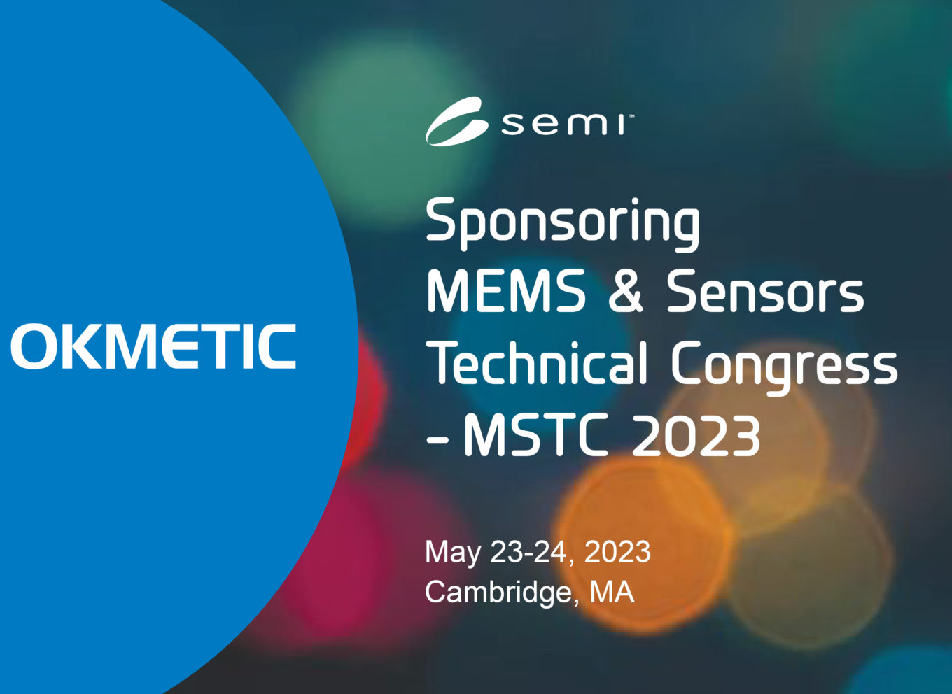
Okmetic is sponsoring the MEMS & Sensors Technical Congress 2023
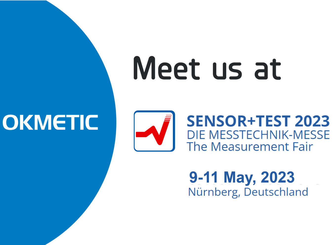
Okmetic is participating in SENSOR+TEST on May 9-11 in Nuremberg
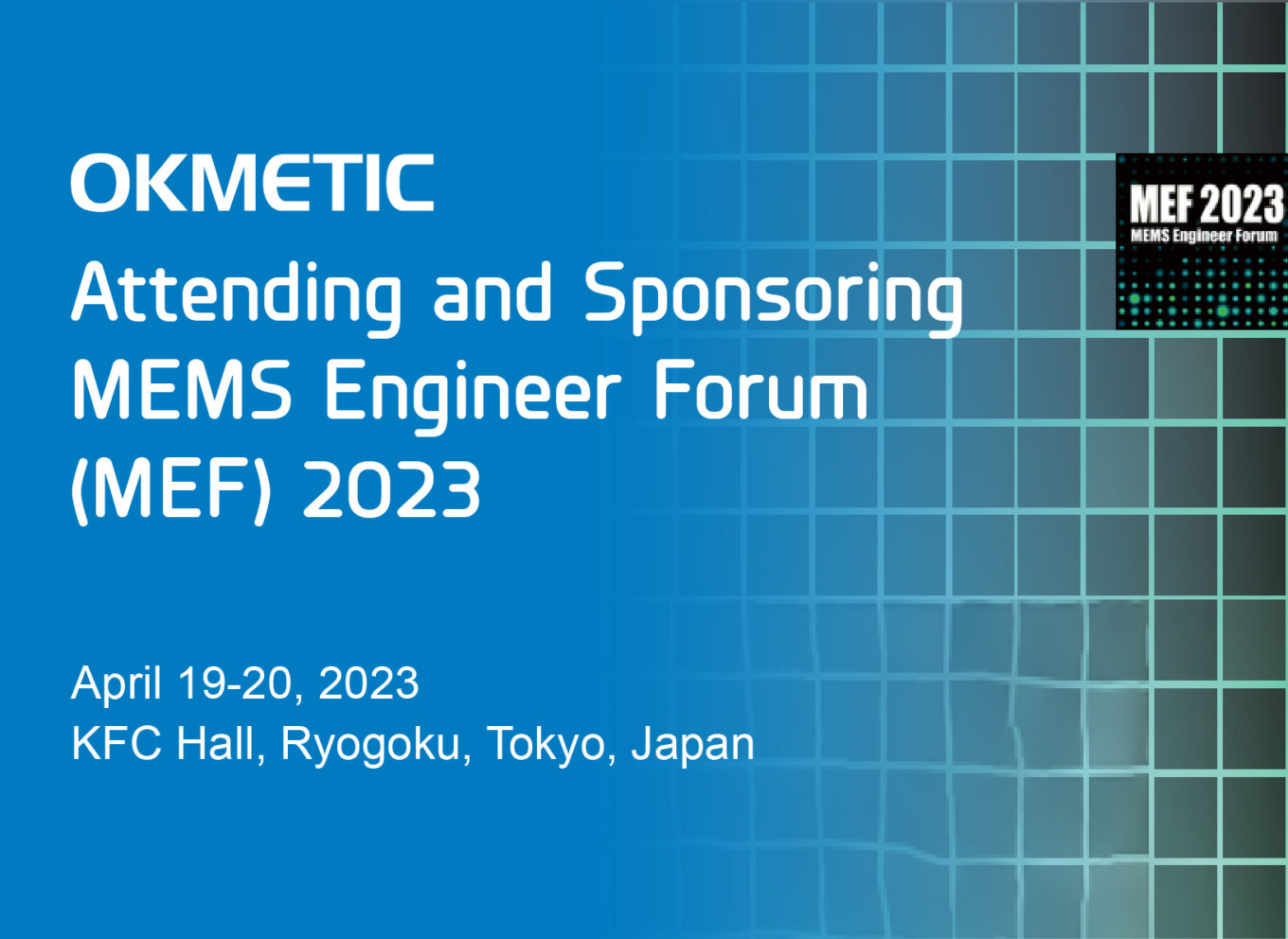
Okmetic is sponsoring and attending MEF 2023 to be held on April 20-21 in Tokyo
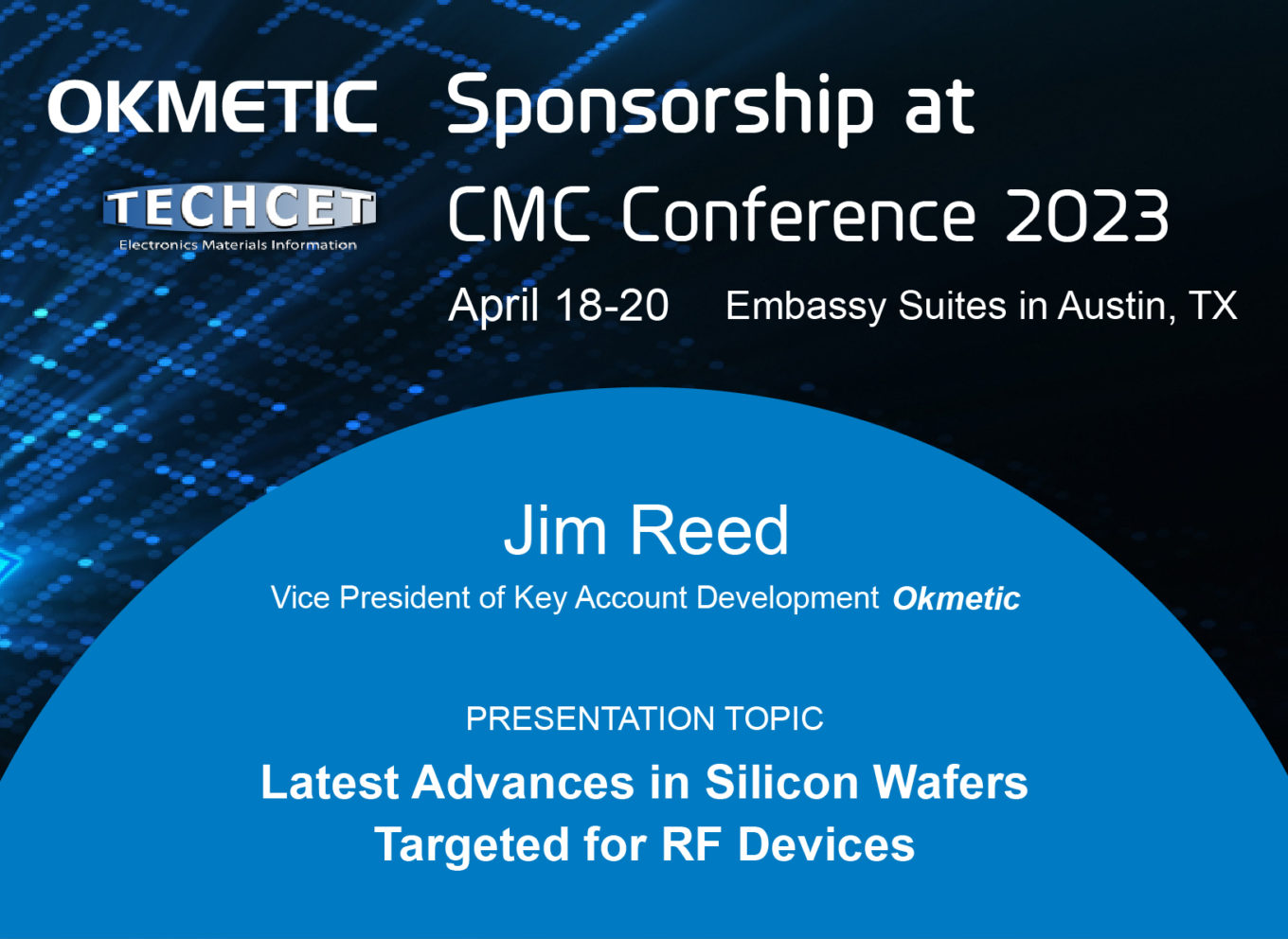
Okmetic’s Vice President of Key Account Development Jim Reed will be giving a speech at CMC Conference 2023

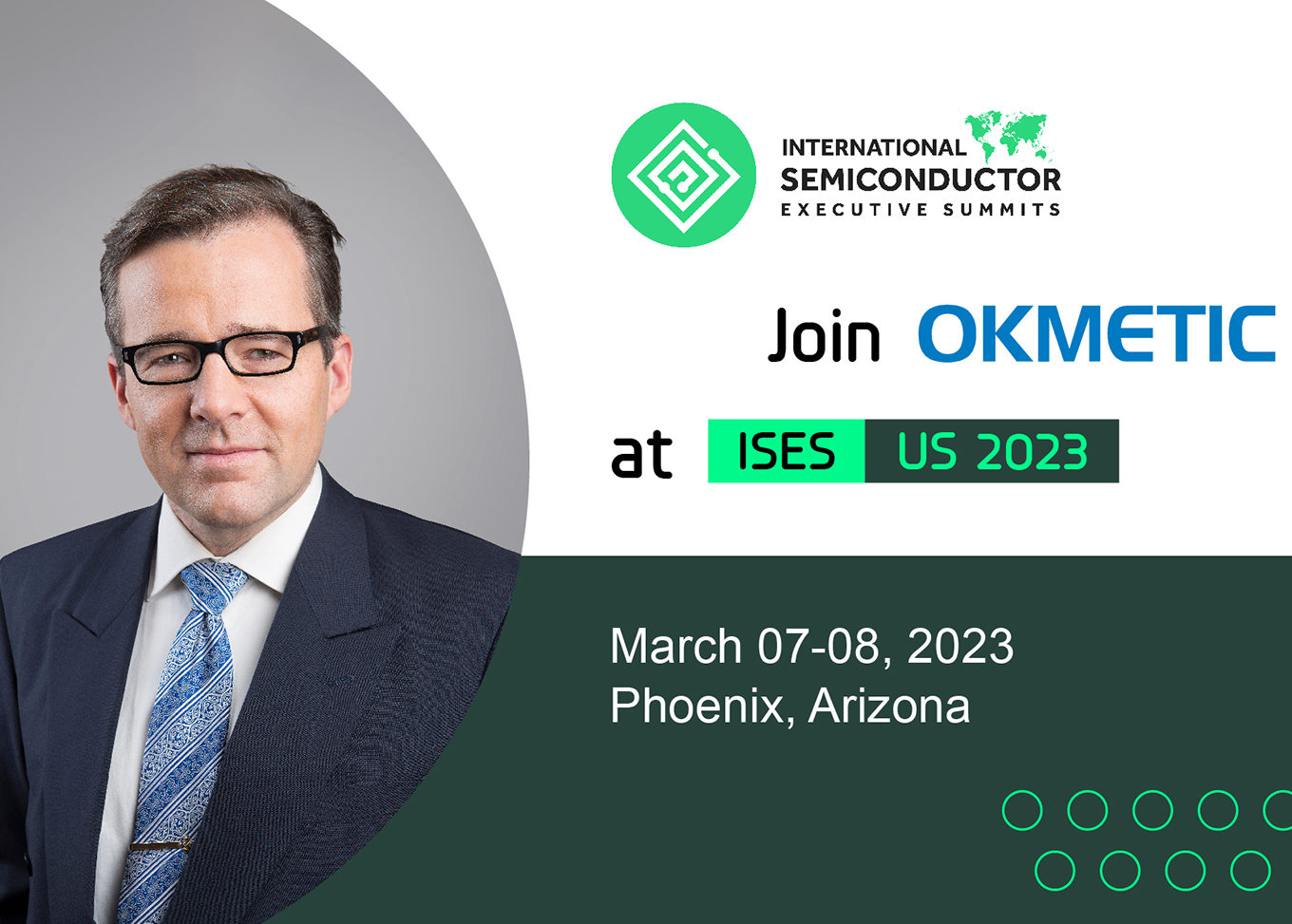
Okmetic is attending APEC 2023 held in Orlando during March 19-23, 2023

Okmetic is part of Semi-Summer 2023 –program